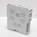
AVMOD IO44D, IO44DU
Application
The modules are designed for discrete control with different load and inquiries for status of discrete inputs through the interface RS485 or USB. Device name has type marking which indicates that digital input/output device has 4 inputs and 4 outputs, and if it contans the "U" letter - device has USB interface with appropriate functionality.
Functional capabilities
- 4 groups of contacts (relay) and 4 discreet inputs;
- Maximum switching current up to 5 A and voltage up to 240 V;
- Galvanically decoupled RS485 and USB 2.0 interfaces;
- Can be used as USB to RS485 converter;
- Ability to connect a number of devices to one bus;
- Control via industry standard ModBus protocol;
- Asynchronous registration of input events;
- Relays can be flipped for a defined time interval by one command;
- Access trough the virtual COM-port when connected to the PC by USB;
- Galvanically decoupled inputs with internal pull-up resistors or independent voltage inputs;
- Reliable and practical enclosure that can be installed on DIN-rail;
- Test and configuration utility for PC is supplied;
- The ability to broadcast the status of inputs to outputs.
Technical characteristics
Parameters of contact pairs
| Number of contact pairs | 4 |
| Maximum switching voltage | 240V |
| Maximum switching current | 5A |
| Galvanic decoupling from other nodes in a circuit | >1000V |
| Mechanical reliability of contacts | 10 000 000 responses |
| Electrical strength of contacts | 10 000 responses |
| Versions of contact pairs | closed/open |
Parameters of discrete inputs
| Number of inputs | 4 |
| Input variants | |
| Commutation to the common ground: | |
| Internal pull-up resistors | 2.2kOm |
| Internal source voltage | +4V |
| Independent isolated voltage-driven inputs | |
| Voltage | +5/+12/+24V |
| Overvoltage protection | <2Unom |
| Galvanic decoupling from other nodes in a circuit | >1000V |
Parameters of RS485 Interface
| Supported baud rate, Bd | 4800, 9600, 14400, 57600, 19200, 38400, 115200 |
| Parity modes | EVEN, ODD, NO |
| Galvanic decoupling from other nodes in a circuit | 1000V |
| ESD protection | 20kV |
Parameters of USB* interface
| Specification | 2.0 |
| Electrostatic discharge protection | 20kV |
| Galvanic decoupling from other nodes in a circuit | >1000V |
Power parameters
| Supply voltage | 10…30V |
| Maximum consumption current | 150mA |
| Power polarity changing protection | Implemented |
*Only for IO44DU module
Connection of external circuits
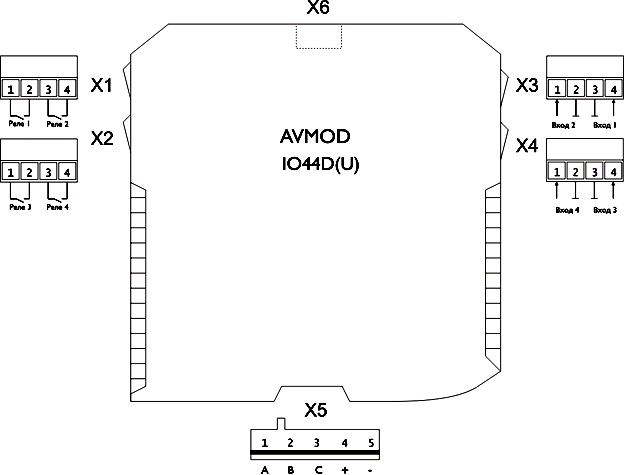
The following is the schema of external connectors of IO44D/IO44DU module:
| Connector | Description | Contacts | ||||
| 1 | 2 | 3 | 4 | 5 | ||
| X1 | Relays 1,2 | Relay 1 | Relay 1 | Relay 2 | Relay 2 | - |
| X2 Relays 3,4 Relay 3 Relay 3 Relay 4 Relay 4 - | ||||||
| X3 Inputs 1,2 Input 2 Input 2 common Input 1 common Input 1 - | ||||||
| X4 Inputs 3,4 Input 4 Input 4 common Input 3 common Input 3 - | ||||||
| X5 RS485, power supply RS485 A RS485 B RS485 C (common) +Usup -Usup | ||||||
| X6* Type B USB slot - | ||||||
SA1 – termination resistor and safe bias resistor switch
*Only for IO44DU module
RS485 interface
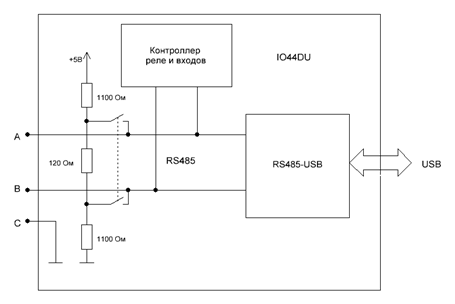
IO44DU
Internal logical structure of IO44DU module is as follows:
Module has internal RS485 bus, to which relay and discrete input controller is connected. Access to RS485 bus can be achieved in two ways: by connecting directly to its lines through device’s outer connectors, or through the built in RS485-USB interface converter (see the “USB interface” section).
When connecting through RS485-RS232 converter port number is being defined by physical number of the COM port, to which converter is connected.
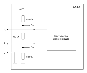
IO44D
Internal logical structure of IO44D module is as follows:
Module control can be performed only with additional interface converter or IO44DU module connected to common RS485 bus.
Attention!
If several IO44D(U) modules are connected to RS485 bus, it is necessary to turn SA1 switch to position “1” on two of them that are topologically placed at the ends of the bus. It is needed for connection of termination resistor and safe bias resistor.
A number of IO44D modules can be connected to RS485 bus, only if each module has a unique address.
Relay contacts
AVMOD modules IO44DU and IO44D contain four galvanically independent relay contact groups brought out to the external terminal blocks. Typical scheme of management of external loads is as follows:
Discrete inputs
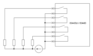
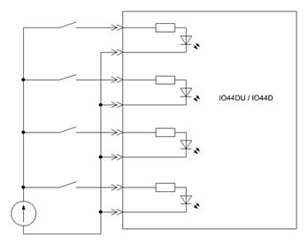
IO44DU/IO44D modules can have two different types of digital inputs. The first type is independent isolated voltage-driven inputs. To feed a logical one to the input, it must be connected to an external power source. Ratings of the internal limiting resistors depend on the input voltage, with which the module works (+5, +12 or +24). In this version, all the inputs are not galvanically connected to each other and to other nodes in the scheme.
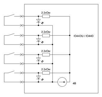
The second version of inputs - the inputs switched to a common ground. To feed a logical one it is necessary to close corresponding input terminals. In this embodiment, the inputs are galvanically decoupled from the rest of circuit nodes, but have a common ground. This embodiment of the inputs is used for conjunction of external keys by "dry contact" scheme.
USB interface (IO44DU)
The USB unit is actually a built-in RS485-USB interface converter, enabling access to the internal RS485 bus of the device. When plugged in USB port, the device is determined by the system as a virtual COM port. Number assigned to the port can be defined as follows: go to Start -> Control Panel -> System -> Hardware -> Device Manager -> Ports COM and LPT. In the list of ports, find the port with the name Silicon Labs CP2103 USB to UART Bridge. Number of this port is the desired one.
Power supply
The module can operate at supply voltages ranging from +10 to +30 V. Recommended operating range is 12 - 24V. Maximum current consumption of the module is 150mA with four relays and supply voltage 10V. Protection against reverse polarity is implemented.
Avmod configuration utility
The tool is designed to configure and test the functionality of various devices of AVMOD series. It makes possible searching for devices connected to the PC serial port (including virtual).
Port selection
To start working with the utility, select the serial port to which the device is connected (see the “USB interface” and “RS485 interface” sections). Port is selected from the “Port” drop-down list, which includes available serial ports.
Search by address
This type of search should be used when one or more modules are connected to the bus, each having equal and known rate of exchange and the type of parity, but different addresses. For search, “by baud rate” and “by address” switches should be turned OFF and ON, respectively. You must also specify the initial (current) and end address, baud rate and parity, in which to search. When searching by the address, baud rate and parity remain unchanged. The search can be carried out until the first device is found, or by the range of addresses.
Search by baud rate
This type of search should be used when the address of the device is known, but exchange rate and the type of parity are unknown. For search, “by baud rate” and “by address” switches should be turned ON and OFF, respectively. The current address should be provided as well. When searching by baud rate, the current address remains unchanged. The search can be carried out until the first device is found, or in all possible combinations of baud rate and parity.
Attention!
When devices with the same address, baud rate, parity, or the same baud rate, and the address, but different parity are connected to a single bus, conflict may arise, leading to incorrect device detection.
Search by baud rate and address
This type of search should be used in case if the address, baud rate and parity of the devices connected to the bus, are unknown. This type of search is the slowest since it implies consistent review of all possible combinations of baud rate and parity for all addresses. For search, “by baud rate” and “by address”, both switches should be turned ON. Initial (current) and end address range should be specified as well. The search can be carried out until the first device is found, or by all addresses for each possible combinations of baud rate and parity.
Device configuration
Configuration of the device is done directly in the device list window. To change the baud rate or the type of device parity, click the appropriate box and select the desired values in the drop-down list. To change the address of the device, enter the desired value into the address cell.
Control mode of IO44D and IO44DU modules
To switch to the control mode, select the device from the device list in the “Search” tab. The “Control” tab will appear. It will contain control elements specific for the selected device type. For these modules the following controls are available:
- Switch of the relay’s state;
- Specified time interval switches of the relay;
- Flags of the input state and their reset button (« <- »);
- Flags that register transitions from 1 to 0 and their update and reset buttons (« <- » and «0» );
- Flags that register transitions from 0 to 1 and their update and reset buttons (« <- » and «0» );
- Flags that register any transitions and their update and reset buttons (« <- » and «0» ).
Terminal display mode
Terminal allows controlling the exchange of packages between the software and modules. To enable the display of the terminal, select Show Terminal in the View menu. To hide the terminal, select Hide the terminal.
Program model of IO44D and IO44DU
Description of the communication protocol
Data exchange happens by means of the packages. Each package consists of one address byte, function code byte, a sequence of data bytes, and two-byte checksum. Functional code and data bytes form the elementary protocol package (PDU).
| Address on bus | Functional code | Data | CRC16 |
Address of the device determines for which device on the bus is the current package or on what device it was obtained (in case of sending a response). The address can be in the range 1...255 (recommended in the protocol specification ModBus addresses are 1...247). Address 0 - broadcast: when referring to it all the devices connected to the bus follow the corresponding instructions, without sending a response package. Packages with address that does not match the address of the device or is not zero, are being ignored by the device. Functional codes define the purpose of the data that follows. The checksum is calculated on the basis of the standard ModBus polynomial. If the checksum does not match, the device ignores the package.
According to the ModBus protocol, access to resources of AVMOD IO44D (U) module is carried out by bit or registers method, i.e. communication with a variety of resources, such as relays or inputs, in most cases, can occur through the read-write binary (bit) variables, and through the ranks of the relevant registers.
Functional codes
The AVMOD IO44DU device supports the following functional codes:
| Functional code | Description |
|---|---|
| 0х01 | reading of bit variables |
| 0х02 | reading of discrete inputs |
| 0х03 | reading of registers |
| 0х05 | writing of one bit variable |
| 0х06 | writing of one register |
| 0х0F | writing of bit variables |
| 0х10 | writing of registers |
0х01 (1) – Allows reading values of several bit variables. The address of the first variable with which to begin reading and the number of variables that should be read are specified in the request. In the response, values of the variables are represented by bits, i.e. first variable corresponds to the first (lower) bit of the low byte, the second - the second bit, etc. The n number of data bytes in the response equals to the number of variables divided by 8 and rounded up to the nearest whole number.
Request:
| Description | Byte | Values range |
|---|---|---|
| Functional code | 1 | 0х01 |
| Start address | 2 | 0x0000 - 0x000F |
| Number of variables | 2 | 0х0001 - 0х000F |
Response:
| Description | Byte | Values range |
|---|---|---|
| Functional code | 1 | 0х01 |
| Number of bytes | 1 | 0x01 - 0x02 |
| Variable values | n | - |
Example: read state of four discrete variables, beginning with address 0х0000 (variables with addresses 0 and 2 - logical 1, 1 and 3 – logical 0)
Request: 01 01 00 00 00 04 3D CD
Response: 01 01 01 05 91 8B
0х02 (2) – Allows reading values of several discrete inputs. The address of the input from which to begin reading and the number of inputs that should be read are specified in the request. In the response, values of the inputs are represented by bits, i.e. first input corresponds to the first (lower) bit of the low byte, the second - the second bit, etc. The n number of data bytes in the response equals to the number of inputs divided by 8 and rounded up to the nearest whole number.
Request:
| Description | Byte | Values range |
|---|---|---|
| Functional code | 1 | 0х02 |
| Start address | 2 | 0x0000 - 0x000F |
| Number of variables | 2 | 0х0001 - 0х0010 |
Response:
| Description | Byte | Values range |
|---|---|---|
| Functional code | 1 | 0х01 |
| Number of bytes | 1 | 0x01 - 0x02 |
| Variable values | n | - |
Example: read state of four discrete inputs, beginning with address 0х0004 (input 4 – logical 1)
Request: 01 02 00 04 00 04 38 08
Response: 01 02 01 08 A0 4E
0х03 (3) – Allows reading of several registers. The address of the first register from which to begin reading and the number of registers that should be read are specified in the request. In the response, two bytes of data correspond to each register.
Request:
| Description | Byte | Values range |
|---|---|---|
| Functional code | 1 | 0х03 |
| Start address | 2 | 0x0000 - 0x000C |
| Number of variables | 2 | 0х0001 - 0х000D |
Response:
| Description | Byte | Values range |
|---|---|---|
| Functional code | 1 | 0х03 |
| Number of bytes | 2 | 0x0001 - 0x000D |
| Number of variables | n | - |
Example: Read the contents of two registers beginning with address 0х0000 (contents 0х0001 and 0х0222)
Request: 01 03 00 00 00 02 C4 0B
Response: 01 03 04 02 22 00 01 9А 41
0х05 (5) – Allows changing of one bit variable at specified address. The variable is being set to logical 1, if passed value equals to 0хFF00 and to logical 0, if 0х0000. All other values lead to generation of the error code.
Request:
| Description | Byte | Values range |
|---|---|---|
| Functional code | 1 | 0х05 |
| Address | 2 | 0x0000 - 0x000F |
| Value | 2 | 0х0000 or 0хFF00 |
Response:
| Description | Byte | Values range |
|---|---|---|
| Functional code | 1 | 0х05 |
| Address | 2 | 0x0000 - 0x000F |
| Value | 2 | 0х0000 or 0хFF00 |
Example: Write logical 1 into variable with address 0х0000.
Request: 01 05 00 00 FF 00 8C 3A
Response: 01 05 00 00 FF 00 8C 3A
0х06 (6) – Allows changing the value of one register at the specified address.
Request:
| Description | Byte | Values range |
|---|---|---|
| Functional code | 1 | 0х06 |
| Address | 2 | 0x0002 - 0x000C |
| Value | 2 | 0х0000 - 0хFFFF |
Response:
| Description | Byte | Values range |
|---|---|---|
| Functional code | 1 | 0х06 |
| Address | 2 | 0x0002 - 0x000 |
| Value | 2 | 0х0000 - 0хFFFF |
Example: Write 0х0010 value into register with address 0х0009.
Request: 01 06 00 09 00 10 58 04
Response: 01 06 00 09 00 10 58 04
0x0F (15) – Allows changing states of several bit variables. The address of the first variable and the number of variable that should be written are specified in the request. Values of the variables are defined by corresponding bits of data bytes, i.e. first variable corresponds to the first (lower) bit of the low byte, the second - the second bit, etc. The n number of data bytes equals to the number of variables divided by 8 and rounded up to the nearest whole number.
Request:
| Description | Byte | Values range |
|---|---|---|
| Functional code | 1 | 0х0F |
| Start address | 2 | 0x0000 - 0x000F |
| Number of variables | 2 | 0х0001 - 0х0010 |
| Number of bytes | 1 | n |
| Value | n | - |
Response:
| Description | Byte | Values range |
|---|---|---|
| Functional code | 1 | 0х0F |
| Start address | 2 | 0x0000 - 0x000F |
| Number of variables | 2 | 0х0001 - 0х0010 |
Example: Write four bit variables beginning with the address 0х0000 (0 and 2 – logical 1)
Request: 01 0F 00 00 00 04 01 05 FE 95
Response: 01 0F 00 00 00 04 54 08
0x10 (16) – Allows changing values of several registers. The address of the first register and the number of registers that should be written are specified in the request. The n number of data bytes should equal to the number of registers multiplied by two.
Request:
| Description | Byte | Values range |
|---|---|---|
| Functional code | 1 | 0х10 |
| Start address | 2 | 0x0002 - 0x000C |
| Number of variables | 2 | 0х0001 - 0х000A |
| Number of bytes | 1 | n |
| Value | n | - |
Response:
| Description | Byte | Values range |
|---|---|---|
| Functional code | 1 | 0х10 |
| Start address | 2 | 0x0002 - 0x000C |
| Number of variables | 2 | 0х0001 - 0х000A |
Example: Write 0х0010 value into four registers beginning with the address 0х0009
Request: 01 10 00 09 00 04 08 00 10 00 10 00 10 00 10 7A 6D
Response: 01 10 00 09 00 04 11 C8
Error codes
If an error occurs while accessing resources on the device, the response package will contain a functional error code and exception code. The error code is formed by adding the function code of request with the 0x80 constant.
Error:
| Description | Byte | Values range |
|---|---|---|
| Functional code | 1 | Functional request code + 0х80 |
| Exception | 1 | 0х01 or 0х02 or 0х03 or 0х04 |
Exception codes indicate the type of error:
- 0х01 – wrong functional code
- 0х02 – wrong data address
- 0х03 – wrong data value
- '0х04 – error while trying to execute function
Description of registers
Access to the registers is carried out with functional codes 0x03, 0x06 and 0x10
| Register address | Description |
|---|---|
| 0x00 | Two upper bytes of serial number |
| 0x01 | Two lower bytes of serial number |
| 0x02 | Device’s address |
| 0x03 | Baud rate/parity |
| 0x04 | Relay (lower nibble) |
| 0x05 | Inputs (lower nibble) |
| 0x06 | Transitions from high to low (lower nibble) |
| 0x07 | Transitions from low to high (lower nibble) |
| 0x08 | Any transitions (lower nibble) |
| 0x09 | Switching relay 1 to the specified number of tenths of a second |
| 0x0A | Switching relay 2 to the specified number of tenths of a second |
| 0x0B | Switching relay 3 to the specified number of tenths of a second |
| 0x0C | Switching relay 4 to the specified number of tenths of a second |
| 0x0D | Link between inputs and outputs |
0x00, 0x01 (read only) – registers, containing type of the device and serial number.
0x02 – device address register on the ModBus.
0x03 – baud rate and parity setting register on the RS485 line.
Lower byte of the register defines baud rate:
| Lower byte of 0x03 register | Baud rate, Bd |
|---|---|
| 0 | 4800 |
| 1 | 9600 |
| 2 | 14400 |
| 3 | 19200* |
| 4 | 38400 |
| 5 | 57600 |
| 6 | 115200 |
High byte determines the type or presence of parity byte in the package:
| High byte of 0x03 register | Parity |
|---|---|
| 0 | EVEN* |
| 1 | ODD |
| 2 | NO |
* Factory baud rate and parity (0x0003).
0x04 – relay control register. Lower nibble bits of this register determine the state of the relay. While writing logical one to the corresponding bit, the contacts are being closed if they were normally opened. In case if they were closed, the contacts will be opened while writing logical one.
0x05 – register of the discrete inputs. Lower nibble of this register correspond to the discrete inputs. In case when pull-up resistors are present, corresponding bit is set to logical one if input is connected to the ground. If pull-up resistors are not present the bit is set when voltage that exceeds threshold appears on the input.
0х06 – latch register, the corresponding bits of which (lower nibble) are set to 1 if on one or more inputs there was a transition from high to low level. Bits can be reset to initial state only with software writing 0.
0х07 – latch register, the corresponding bits of which (lower nibble) are set to 1 if on one or more inputs there was a transition from low to high level. Bits can be reset to initial state only with software writing 0.
0х08 – latch register, the corresponding bits of which (lower nibble) are set to 1 if on one or more inputs there was any transition of state. Bits can be reset to initial state only with software writing 0.
0х09, 0х0A, 0x0B, 0x0C – 2-byte registers that change state of the corresponding relay (0x09 corresponds to relay 1 etc.) for specified time interval. When writing to a register with number N different from 0, the state of the relay switches to opposite for the specified by the written number time period. The number has a dimension of tenth of a second, i.e. T (time delay) in seconds can be defined by the formula T = N * 10. After specified time delay, the relay switches to its original state.
0x0D – discrete inputs and relay linking register. When setting register’s bits of lower nibble to 1, connection between corresponding inputs and outputs is being established.
Bit variables and inputs
Access to bit variables is carried out with functional codes 0x01, 0x05, 0x0F; to discrete inputs – 0x02
| Address | Description | |
|---|---|---|
| Bit variables | Inputs | |
| 0x00 | Relay 1 | Input 1 |
| 0x01 | Relay 2 | Input 2 |
| 0x02 | Relay 3 | Input 3 |
| 0x03 | Relay 4 | Input 4 |
| 0x04 | Transition H-L input 1 | Transition H-L input 1 |
| 0x05 | Transition H-L input 2 | Transition H-L input 2 |
| 0x06 | Transition H-L input 3 | Transition H-L input 3 |
| 0x07 | Transition H-L input 4 | Transition H-L input 4 |
| 0x08 | Transition L-H input 1 | Transition L-H input 1 |
| 0x09 | Transition L-H input 2 | Transition L-H input 2 |
| 0x0A | Transition L-H input 3 | Transition L-H input 3 |
| 0x0B | Transition L-H input 4 | Transition L-H input 4 |
| 0x0C | Any transition input 1 | Any transition input 1 |
| 0x0D | Any transition input 2 | Any transition input 2 |
| 0x0E | Any transition input 3 | Any transition input 3 |
| 0x0F | Any transition input 4 | Any transition input 4 |
| 0x10 | Linking of input 1 with relay 1 | Linking of input 1 with relay 1 |
| 0x11 | Linking of input 2 with relay 2 | Linking of input 2 with relay 2 |
| 0x12 | Linking of input 3 with relay 3 | Linking of input 3 with relay 3 |
| 0x13 | Linking of input 4 with relay 4 | Linking of input 4 with relay 4 |
0x00, 0х01, 0x02, 0x03 – discrete variables of relays or inputs. Functional codes 0x01, 0x05, 0x0F correspond to bits of first nibble of register 0x04 (relay). Code 0x02 allows reading state of the corresponding inputs.
0x04, 0х05, 0x06, 0x07 – correspond to the first four bits of the latch resistor’s transition from high to low level (0x06). Available by functional codes 0x01, 0x02, 0x05, 0x0F.
0x08, 0х09, 0x0A, 0x0B – correspond to the first four bits of the latch resistor’s transition from low to high level (0х07). Available by functional codes 0x01, 0x02, 0x05, 0x0F.
0x0C, 0х0D, 0x0E, 0x0F – correspond to the first four bits of the latch resistor’s transition from high to low level (0х08). Available by functional codes 0x01, 0x02, 0x05, 0x0F.
0x10, 0х11, 0x12, 0x13 – correspond to the first four bits of input and relay linking register (0х0D). Available by functional codes 0x01, 0x02, 0x05, 0x0F.
Example of checksum calculation subprogram in C
unsigned char auchCRCHi[] = {
0x00, 0xC1, 0x81, 0x40, 0x01, 0xC0, 0x80, 0x41, 0x01, 0xC0, 0x80, 0x41, 0x00, 0xC1, 0x81,
0x40, 0x01, 0xC0, 0x80, 0x41, 0x00, 0xC1, 0x81, 0x40, 0x00, 0xC1, 0x81, 0x40, 0x01, 0xC0,
0x80, 0x41, 0x01, 0xC0, 0x80, 0x41, 0x00, 0xC1, 0x81, 0x40, 0x00, 0xC1, 0x81, 0x40, 0x01,
0xC0, 0x80, 0x41, 0x00, 0xC1, 0x81, 0x40, 0x01, 0xC0, 0x80, 0x41, 0x01, 0xC0, 0x80, 0x41,
0x00, 0xC1, 0x81, 0x40, 0x01, 0xC0, 0x80, 0x41, 0x00, 0xC1, 0x81, 0x40, 0x00, 0xC1, 0x81,
0x40, 0x01, 0xC0, 0x80, 0x41, 0x00, 0xC1, 0x81, 0x40, 0x01, 0xC0, 0x80, 0x41, 0x01, 0xC0,
0x80, 0x41, 0x00, 0xC1, 0x81, 0x40, 0x00, 0xC1, 0x81, 0x40, 0x01, 0xC0, 0x80, 0x41, 0x01,
0xC0, 0x80, 0x41, 0x00, 0xC1, 0x81, 0x40, 0x01, 0xC0, 0x80, 0x41, 0x00, 0xC1, 0x81, 0x40,
0x00, 0xC1, 0x81, 0x40, 0x01, 0xC0, 0x80, 0x41, 0x01, 0xC0, 0x80, 0x41, 0x00, 0xC1, 0x81,
0x40, 0x00, 0xC1, 0x81, 0x40, 0x01, 0xC0, 0x80, 0x41, 0x00, 0xC1, 0x81, 0x40, 0x01, 0xC0,
0x80, 0x41, 0x01, 0xC0, 0x80, 0x41, 0x00, 0xC1, 0x81, 0x40, 0x00, 0xC1, 0x81, 0x40, 0x01,
0xC0, 0x80, 0x41, 0x01, 0xC0, 0x80, 0x41, 0x00, 0xC1, 0x81, 0x40, 0x01, 0xC0, 0x80, 0x41,
0x00, 0xC1, 0x81, 0x40, 0x00, 0xC1, 0x81, 0x40, 0x01, 0xC0, 0x80, 0x41, 0x00, 0xC1, 0x81,
0x40, 0x01, 0xC0, 0x80, 0x41, 0x01, 0xC0, 0x80, 0x41, 0x00, 0xC1, 0x81, 0x40, 0x01, 0xC0,
0x80, 0x41, 0x00, 0xC1, 0x81, 0x40, 0x00, 0xC1, 0x81, 0x40, 0x01, 0xC0, 0x80, 0x41, 0x01,
0xC0, 0x80, 0x41, 0x00, 0xC1, 0x81, 0x40, 0x00, 0xC1, 0x81, 0x40, 0x01, 0xC0, 0x80, 0x41,
0x00, 0xC1, 0x81, 0x40, 0x01, 0xC0, 0x80, 0x41, 0x01, 0xC0, 0x80, 0x41, 0x00, 0xC1, 0x81,
0x40
} ;

unsigned char auchCRCLo[] = {
0x00, 0xC0, 0xC1, 0x01, 0xC3, 0x03, 0x02, 0xC2, 0xC6, 0x06, 0x07, 0xC7, 0x05, 0xC5, 0xC4,
0x04, 0xCC, 0x0C, 0x0D, 0xCD, 0x0F, 0xCF, 0xCE, 0x0E, 0x0A, 0xCA, 0xCB, 0x0B, 0xC9, 0x09,
0x08, 0xC8, 0xD8, 0x18, 0x19, 0xD9, 0x1B, 0xDB, 0xDA, 0x1A, 0x1E, 0xDE, 0xDF, 0x1F, 0xDD,
0x1D, 0x1C, 0xDC, 0x14, 0xD4, 0xD5, 0x15, 0xD7, 0x17, 0x16, 0xD6, 0xD2, 0x12, 0x13, 0xD3,
0x11, 0xD1, 0xD0, 0x10, 0xF0, 0x30, 0x31, 0xF1, 0x33, 0xF3, 0xF2, 0x32, 0x36, 0xF6, 0xF7,
0x37, 0xF5, 0x35, 0x34, 0xF4, 0x3C, 0xFC, 0xFD, 0x3D, 0xFF, 0x3F, 0x3E, 0xFE, 0xFA, 0x3A,
0x3B, 0xFB, 0x39, 0xF9, 0xF8, 0x38, 0x28, 0xE8, 0xE9, 0x29, 0xEB, 0x2B, 0x2A, 0xEA, 0xEE,
0x2E, 0x2F, 0xEF, 0x2D, 0xED, 0xEC, 0x2C, 0xE4, 0x24, 0x25, 0xE5, 0x27, 0xE7, 0xE6, 0x26,
0x22, 0xE2, 0xE3, 0x23, 0xE1, 0x21, 0x20, 0xE0, 0xA0, 0x60, 0x61, 0xA1, 0x63, 0xA3, 0xA2,
0x62, 0x66, 0xA6, 0xA7, 0x67, 0xA5, 0x65, 0x64, 0xA4, 0x6C, 0xAC, 0xAD, 0x6D, 0xAF, 0x6F,
0x6E, 0xAE, 0xAA, 0x6A, 0x6B, 0xAB, 0x69, 0xA9, 0xA8, 0x68, 0x78, 0xB8, 0xB9, 0x79, 0xBB,
0x7B, 0x7A, 0xBA, 0xBE, 0x7E, 0x7F, 0xBF, 0x7D, 0xBD, 0xBC, 0x7C, 0xB4, 0x74, 0x75, 0xB5,
0x77, 0xB7, 0xB6, 0x76, 0x72, 0xB2, 0xB3, 0x73, 0xB1, 0x71, 0x70, 0xB0, 0x50, 0x90, 0x91,
0x51, 0x93, 0x53, 0x52, 0x92, 0x96, 0x56, 0x57, 0x97, 0x55, 0x95, 0x94, 0x54, 0x9C, 0x5C,
0x5D, 0x9D, 0x5F, 0x9F, 0x9E, 0x5E, 0x5A, 0x9A, 0x9B, 0x5B, 0x99, 0x59, 0x58, 0x98, 0x88,
0x48, 0x49, 0x89, 0x4B, 0x8B, 0x8A, 0x4A, 0x4E, 0x8E, 0x8F, 0x4F, 0x8D, 0x4D, 0x4C, 0x8C,
0x44, 0x84, 0x85, 0x45, 0x87, 0x47, 0x46, 0x86, 0x82, 0x42, 0x43, 0x83, 0x41, 0x81, 0x80,
0x40
};

unsigned short CRC16 ( unsigned char *puchMsg, unsigned short usDataLen)
{
	unsigned char uchCRCHi = 0xFF ;
	unsigned char uchCRCLo = 0xFF ;
	unsigned uIndex ;
	while (usDataLen--) {
		uIndex = uchCRCLo ^ *puchMsg++ ;
		uchCRCLo = uchCRCHi ^ auchCRCHi[uIndex] ;
		uchCRCHi = auchCRCLo[uIndex] ;
	}
	return (uchCRCHi << 8 | uchCRCLo) ;
}
Example of checksum calculation subprogram in Pascal
const

CRChi : array[0..255] of byte =
  (
  $00,$C1,$81,$40,$01,$C0,$80,$41,$01,$C0,$80,$41,$00,$C1,$81,$40,
  $01,$C0,$80,$41,$00,$C1,$81,$40,$00,$C1,$81,$40,$01,$C0,$80,$41,
  $01,$C0,$80,$41,$00,$C1,$81,$40,$00,$C1,$81,$40,$01,$C0,$80,$41,
  $00,$C1,$81,$40,$01,$C0,$80,$41,$01,$C0,$80,$41,$00,$C1,$81,$40,
  $01,$C0,$80,$41,$00,$C1,$81,$40,$00,$C1,$81,$40,$01,$C0,$80,$41,
  $00,$C1,$81,$40,$01,$C0,$80,$41,$01,$C0,$80,$41,$00,$C1,$81,$40,
  $00,$C1,$81,$40,$01,$C0,$80,$41,$01,$C0,$80,$41,$00,$C1,$81,$40,
  $01,$C0,$80,$41,$00,$C1,$81,$40,$00,$C1,$81,$40,$01,$C0,$80,$41,
  $01,$C0,$80,$41,$00,$C1,$81,$40,$00,$C1,$81,$40,$01,$C0,$80,$41,
  $00,$C1,$81,$40,$01,$C0,$80,$41,$01,$C0,$80,$41,$00,$C1,$81,$40,
  $00,$C1,$81,$40,$01,$C0,$80,$41,$01,$C0,$80,$41,$00,$C1,$81,$40,
  $01,$C0,$80,$41,$00,$C1,$81,$40,$00,$C1,$81,$40,$01,$C0,$80,$41,
  $00,$C1,$81,$40,$01,$C0,$80,$41,$01,$C0,$80,$41,$00,$C1,$81,$40,
  $01,$C0,$80,$41,$00,$C1,$81,$40,$00,$C1,$81,$40,$01,$C0,$80,$41,
  $01,$C0,$80,$41,$00,$C1,$81,$40,$00,$C1,$81,$40,$01,$C0,$80,$41,
  $00,$C1,$81,$40,$01,$C0,$80,$41,$01,$C0,$80,$41,$00,$C1,$81,$40 );

CRClo : array[0..255] of byte =
  (
  $00,$C0,$C1,$01,$C3,$03,$02,$C2,$C6,$06,$07,$C7,$05,$C5,$C4,$04,
  $CC,$0C,$0D,$CD,$0F,$CF,$CE,$0E,$0A,$CA,$CB,$0B,$C9,$09,$08,$C8,
  $D8,$18,$19,$D9,$1B,$DB,$DA,$1A,$1E,$DE,$DF,$1F,$DD,$1D,$1C,$DC,
  $14,$D4,$D5,$15,$D7,$17,$16,$D6,$D2,$12,$13,$D3,$11,$D1,$D0,$10,
  $F0,$30,$31,$F1,$33,$F3,$F2,$32,$36,$F6,$F7,$37,$F5,$35,$34,$F4,
  $3C,$FC,$FD,$3D,$FF,$3F,$3E,$FE,$FA,$3A,$3B,$FB,$39,$F9,$F8,$38,
  $28,$E8,$E9,$29,$EB,$2B,$2A,$EA,$EE,$2E,$2F,$EF,$2D,$ED,$EC,$2C,
  $E4,$24,$25,$E5,$27,$E7,$E6,$26,$22,$E2,$E3,$23,$E1,$21,$20,$E0,
  $A0,$60,$61,$A1,$63,$A3,$A2,$62,$66,$A6,$A7,$67,$A5,$65,$64,$A4,
  $6C,$AC,$AD,$6D,$AF,$6F,$6E,$AE,$AA,$6A,$6B,$AB,$69,$A9,$A8,$68,
  $78,$B8,$B9,$79,$BB,$7B,$7A,$BA,$BE,$7E,$7F,$BF,$7D,$BD,$BC,$7C,
  $B4,$74,$75,$B5,$77,$B7,$B6,$76,$72,$B2,$B3,$73,$B1,$71,$70,$B0,
  $50,$90,$91,$51,$93,$53,$52,$92,$96,$56,$57,$97,$55,$95,$94,$54,
  $9C,$5C,$5D,$9D,$5F,$9F,$9E,$5E,$5A,$9A,$9B,$5B,$99,$59,$58,$98,
  $88,$48,$49,$89,$4B,$8B,$8A,$4A,$4E,$8E,$8F,$4F,$8D,$4D,$4C,$8C,
  $44,$84,$85,$45,$87,$47,$46,$86,$82,$42,$43,$83,$41,$81,$80,$40 );


procedure CRC16(Data: array of byte;  len : word; var Hi : byte; var Lo : byte);
var Index : word;
    i : word;
begin
   Hi:=$FF;
   Lo:=$FF;
   i:=0;
   While (i<Len) do
   begin
     Index:=Hi xor Data[i];
     Hi:=Lo xor CRCHi[Index];
       Lo:=CRCLo[Index];
       i:=i+1;
   end;
end;